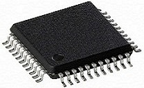
BQFP四方扁平式封装集成电路
该封装的集成电路四周均有引脚,引脚之间距离很小,管脚很细,一般大规模或超大型集成电路都采用这种封装形式。具有性能良好,可靠性高,价格低廉等优势 同时用这种形式封装的集成电路必须采用SMT(表面组装技术)将封装的集成电路与主板焊接起来。采用SMT安装的芯片不必在主板上打孔,一般在主板表面上有设计好的相应管脚的焊点。将各脚对准相应的焊点,即可实现与主板的焊接。
产品特点
1. 适合高频使用
2. 操作方便
3. 工艺成熟
4. 价格便宜
5. 带有缓冲垫,不易损坏
封装结构图
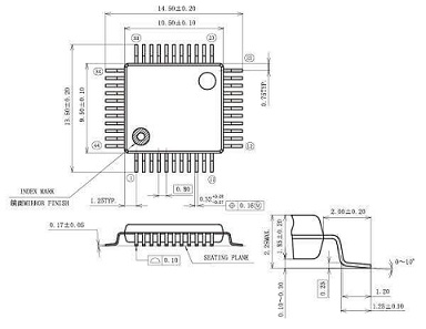
引脚参数
| PIN | SIGNAL | DESCRIPTION |
| 1 | NC | - |
| 2 | A10 | Address input |
| 3 | A8 | Address input |
| 4 | A7 | Address input |
| 5 | A6 | Address input |
| 6 | A5 | Address input |
| 7 | A4 | Address input |
| 8 | A3 | Address input |
| 9 | A2 | Address input |
| 10 | A1 | Address input |
| 11 | A0 | Address input |
| 12 | NC | - |
| 13 | I/O(0) | Data Input/Output |
| 14 | I/O(1) | Data Input/Output |
| 15 | I/O(2) | Data Input/Output |
| 16 | Vss | Ground |
| 17 | I/O(3) | - |
| 18 | I/O(4) | Data Input/Output |
| 19 | I/O(5) | Data Input/Output |
| 20 | I/O(6) | Data Input/Output |
| 21 | I/O(7) | Data Input/Output |
| 22 | I/O(8) | Data Input/Output |
| 23 | CE | Chip Enable |
| 24 | A9 | Address input |
| 25 | OE | Output Enable |
| 26 | NC | - |
| 27 | Vcc | +3.3V |
| 28 | WE | Write Enable |
| 29 | A11 | Address input |
| 30 | CE | Chip Enable |
| 31 | A12 | Address input |
| 32 | A13 | Address input |
| 33 | OE | Output Enable |
| 34 | A14 | Address input |
| 35 | A15 | Address input |
| 36 | A16 | Address input |
| 37 | A17 | Address input |
| 38 | A18 | Address input |
| 39 | Vcc | +3.3v |
| 40 | Vss | Ground |
| 41 | A19 | Address input |
| 42 | CN | - |
| 43 | WE | Write Enable |
| 44 | A20 | Address input |