- Home
- Product
- VCSEL laser chip
- V25-850C series High speed VCESL chip
V25-850C series High speed VCESL chip
The chip is designed with GaAs based vertical cavity surface, multiple emission channels, high transmission rate and high stability, and VCSEL is contacted on the top surface by using ground source (GS) microprobe, wire bonding or flip chip bonding alone. So the chip can be used as an engineering sample to develop and evaluate optical interconnection, optical backplane and integrated waveguide.
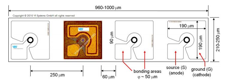
Chip Size
Features
1. Up to 12 parallel channels
2. Up to 28 Gbit/s per channel
3. High temperature stability
4. Device-to-device pitch of 250 µm
Product Parameters
| Parameter | Typical |
| Emission wavelength | 850nm(available 835-865nm) |
| Data rate | Up to 28 Gbit/s |
| Threshold current | < 1 mA |
| Peak output power | 4 mW |
Electro-optical Properties
| Parameter | Symbol | Test Condition | Min | Typ | Max | Unit |
| Emission wavelength | λ | 835 | 865 | nm | ||
| Maximum data rate | Gbps | NRZ | 25 | 28 | Gbit/s | |
| Bandwidth | BW | f(3dB) | 15GHz at 85°C | 18 | GHz | |
| Threshold current | I(th) | I(op) = 5mA | 0.4 | 0.5 | 1 | mA |
| Operating current | V(op) | I(op) = 5mA | 2.3 | 2.5 | 2.7 | V |
| Slope efficiency | η | I(op) = 5mA | 0.3 | 0.45 | W/A | |
| Differential resistance | Rd | I(op) = 5mA | 65 | 75 | 85 | Ω |
| Optical output power | P(op) | 1.5 | 2.5 | 4 | mW | |
| Beam divergence | θ | FWHM | 18 | 20 | 25 | deg |
| Spectral bandwidth (RMS) | ∆λRMS | I(op)= 5mA | 0.4 | 0.6 | nm | |
| Rise / Fall time | τR / τF | 20%-80% | 16 | 20 | ps | |
| Relative intensity noise | RIN | -128 | dB/Hz | |||
| Wavelength tuning over current | 0.3 | nm/mA | ||||
| Wavelength tuning over temp | 0.07 | nm/K | ||||
| Thermal impedance | Z(Thermal) | 2 | °C/mW |