Service Area
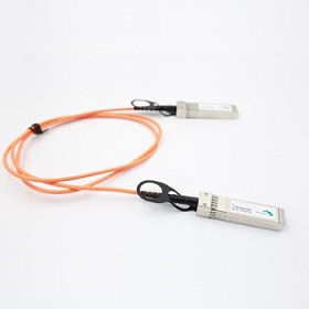
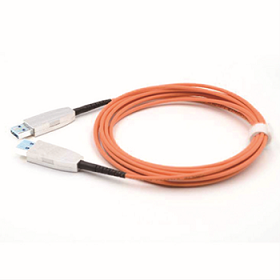
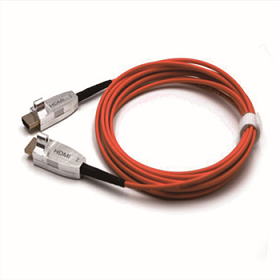
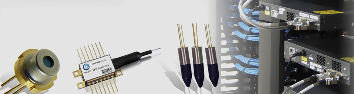
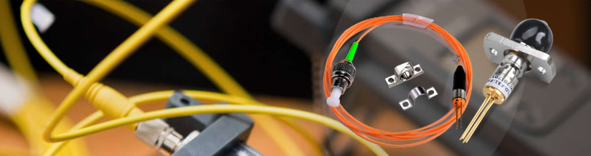
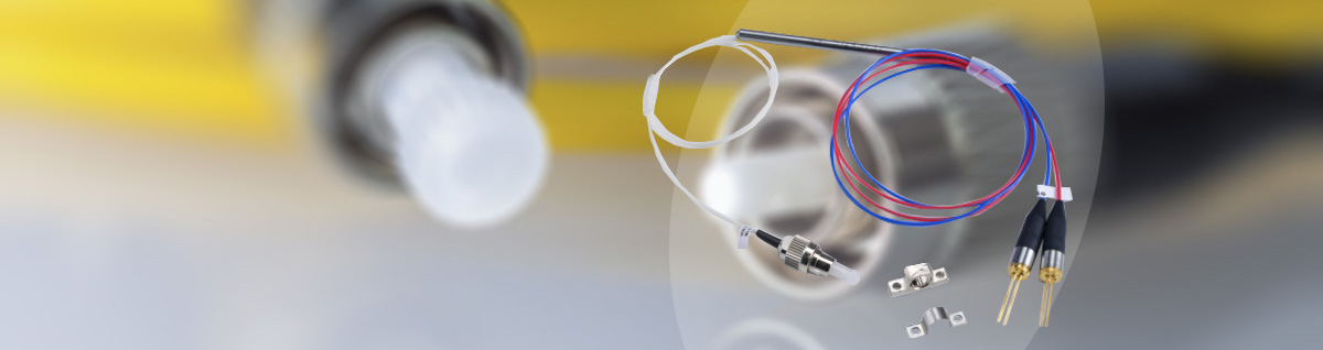
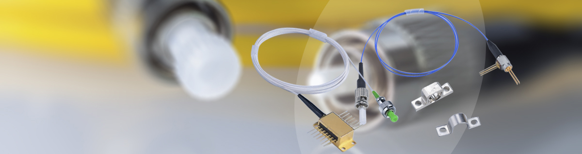
Our company is a professional optoelectronic device manufacturer and supplier in China. We provide integrated circuit, VCSEL laser chip, photoelectric engine device, photoelectric active optical cable device, etc.
-
-
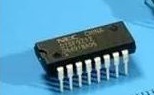
- Dip dual in line package integrated circuitThis packaging method is the earliest IC packaging technology. It has the advantages of excellent performance and high reliability. It is suitable for perforation welding on PCB. It has good compatibility with motherboard and is easy to operate. The application range includes standard logic IC, memory, microcomputer circuit and other integrated circuits.
-
-
-
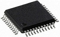
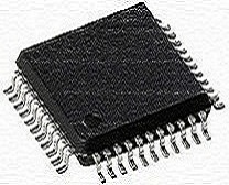
- BQFP quad flatpack integrated circuitThe integrated circuit of this package has pins all around, the distance between the pins is very small, and the pins are very thin. Generally, this kind of package is used in large-scale or ultra large-scale integrated circuits. It has the advantages of good performance, high reliability and low price.
-
-
-

- PLCC package integrated circuit The form of the package is designed for the integrated circuit package without pins. The package adopts the chip type package, the pins of which are bent inward at the edge of the chip, close to the chip, reducing the installation volume and high reliability. The application range includes precision instruments and high frequency equipment.
-
-
-
- VM50-850C series high speed VCSEL chip The VCSEL chip and 1xn (n = 4,12) array can be used as sample backplane, integrated waveguide and next generation optical data communication system for the development and evaluation of engineering application optical interconnection.
-
-
-
- D30-850C high speed VCSEL chip These high-speed top-illuminated GaAs-based pin photodetector chips are available for the usein development and evaluation of lasers and the next-generation of data communicationssystems. The chip exhibits a responsivity greater than 0.4 A/W at 850 nm.
-
-
-

- V25-850C series High speed VCESL chip The chip is designed with GaAs based vertical cavity surface, multiple emission channels, high transmission rate and high stability. So the chip can be used as an engineering sample to develop and evaluate optical interconnection, optical backplane and integrated waveguide.
-