- Home
- Product
- Integrated circuit module device
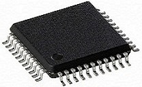
- BQFP quad flatpack integrated circuit
BQFP quad flatpack integrated circuit
The integrated circuit of this package has pins all around, the distance between the pins is very small, and the pins are very thin. Generally, this kind of package is used in large-scale or ultra large-scale integrated circuits. The SMT (surface mount technology) must be used to weld the integrated circuit with the main board. SMT chips do not need to be punched on the motherboard, and there are generally designed solder joints of corresponding pins on the motherboard surface. The welding with the main board can be realized by aligning the feet with the corresponding welding points.
Features
1. Suitable for high frequency use
2. Easy operation
3. Process maturity
4. Cheapness
5. With cushion, not easy to damage
Packaging Structure Diagram
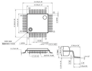
Pin Parameter
| PIN | SIGNAL | DESCRIPTION |
| 1 | NC | - |
| 2 | A10 | Address input |
| 3 | A8 | Address input |
| 4 | A7 | Address input |
| 5 | A6 | Address input |
| 6 | A5 | Address input |
| 7 | A4 | Address input |
| 8 | A3 | Address input |
| 9 | A2 | Address input |
| 10 | A1 | Address input |
| 11 | A0 | Address input |
| 12 | NC | - |
| 13 | I/O(0) | Data Input/Output |
| 14 | I/O(1) | Data Input/Output |
| 15 | I/O(2) | Data Input/Output |
| 16 | Vss | Ground |
| 17 | I/O(3) | - |
| 18 | I/O(4) | Data Input/Output |
| 19 | I/O(5) | Data Input/Output |
| 20 | I/O(6) | Data Input/Output |
| 21 | I/O(7) | Data Input/Output |
| 22 | I/O(8) | Data Input/Output |
| 23 | CE | Chip Enable |
| 24 | A9 | Address input |
| 25 | OE | Output Enable |
| 26 | NC | - |
| 27 | Vcc | +3.3V |
| 28 | WE | Write Enable |
| 29 | A11 | Address input |
| 30 | CE | Chip Enable |
| 31 | A12 | Address input |
| 32 | A13 | Address input |
| 33 | OE | Output Enable |
| 34 | A14 | Address input |
| 35 | A15 | Address input |
| 36 | A16 | Address input |
| 37 | A17 | Address input |
| 38 | A18 | Address input |
| 39 | Vcc | +3.3v |
| 40 | Vss | Ground |
| 41 | A19 | Address input |
| 42 | CN | - |
| 43 | WE | Write Enable |
| 44 | A20 | Address input |