- Home
- Product
- Integrated circuit module device
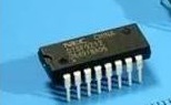
- Dip dual in line package integrated circuit
Dip dual in line package integrated circuit
This packaging method is the earliest IC packaging technology. There are two kinds of packaging materials, ceramic and plastic. It has the advantages of excellent performance and high reliability. It is suitable for punching and welding on PCB. It has good compatibility with the main board. It is easy to operate. It is suitable for small chips without too many wires. The number of pins is generally no more than 100. The integrated circuit with dip packaging has two rows of pins Insert into the chip socket with dip structure. Of course, it can also be directly inserted in the circuit board with the same number of welding holes and geometric arrangement for welding. Take special care when plugging and unplugging from the chip socket to avoid damaging the pins. The application range includes standard logic IC, memory, microcomputer circuit and other integrated circuits.
Features
1. It is suitable for punching and welding on PCB , easy to operate
2. The ratio between chip area and package area is large
3. High reliability
4. Compatible with most motherboard devices
Packaging Structure Diagram
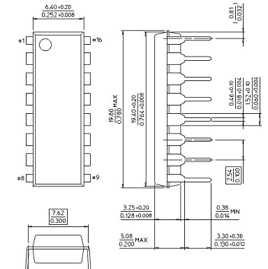
Pin Parameter
| PIN | SIGNAL | DESCRIPTION |
| 1 | GND | Ground |
| 2 | N.C. | - |
| 3 | N.C. | - |
| 4 | GND | Ground |
| 5 | SDA | I2C Data |
| 6 | GND | Ground |
| 7 | SCL | I2C Clock |
| 8 | GND | Ground |
| 9 | N.C. | - |
| 10 | VDD | 3.0V Power |
| 11 | VCC | 3.0V Power |
| 12 | N.C. | - |
| 13 | VCC | 3.0V Power |
| 14 | GND | Ground |
| 15 | SDA | I2C Data |
| 16 | SCL | I2C Clock |