- Home
- Product
- Integrated circuit module device
- PLCC package integrated circuit
PLCC package integrated circuit
The form of the package is designed for the integrated circuit package without pins. The main external material is plastic. This package adopts the chip type package, and its pins bend inward at the edge of the chip, clinging to the chip, reducing the volume and high reliability. But the disadvantage of this kind of chip is that it is very troublesome to debug and weld when it is used. In general, it is not directly welded to the printed circuit board when it is designed, but the pin conversion seat of PGA package structure is welded to the printed circuit board, and then the chip of PLCC package is installed in the installation slot of PLCC structure of the pin conversion seat, so the chip can be disassembled at any time, which is convenient for debugging. The application range includes precision instruments and high frequency equipment.

Features
1. High reliability
2. Small size
3. Demonstrate compact solution scale
4. Fully assembled and tested
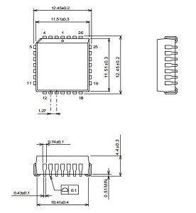
Packaging Structure Diagram
Pin Parameter
| PIN | SIGNAL | DESCRIPTION |
| 1 | NC | - |
| 2 | A10 | Address input |
| 3 | A8 | Address input |
| 4 | A7 | Address input |
| 5 | A6 | Address input |
| 6 | A5 | Address input |
| 7 | A4 | Address input |
| 8 | A3 | Address input |
| 9 | A2 | Address input |
| 10 | A1 | Address input |
| 11 | A0 | Address input |
| 12 | NC | - |
| 13 | I/O(0) | Data Input/Output |
| 14 | I/O(1) | Data Input/Output |
| 15 | I/O(2) | Data Input/Output |
| 16 | Vss | Ground |
| 17 | NC | - |
| 18 | I/O(3) | Data Input/Output |
| 19 | I/O(4) | Data Input/Output |
| 20 | I/O(5) | Data Input/Output |
| 21 | I/O(6) | Data Input/Output |
| 22 | I/O(7) | Data Input/Output |
| 23 | CE | Chip Enable |
| 24 | A9 | Address input |
| 25 | OE | Output Enable |
| 26 | NC | - |
| 27 | Vcc | +5V |
| 28 | WE | Write Enable |